Nanoscience Overview
Nanoscience and Nanotechnology are emerging disciplines that seek to understand the nanoscale processes that govern a material’s behavior. The new directions which are emerging include:
- Preparation and study of novel micro- and nanostructures such as quantum dots and lines
- Combinatorial searches for new superconductors
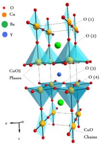
- Exploration of complex oxide systems.
Research Topics
Our group covers a wide array of topics.
- Neuromorphic Computing
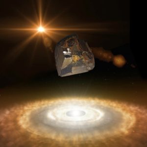
- Extraterrestrial Superconductors
- Synthetic Superconductors
- Phthalocyanine
- Superconducting Vortices
- Complex Oxides
- Exchange Bias
In the News
14.04.2021
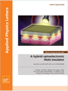
A recent paper entitled “A hybrid optoelectronic Mott insulator” has…
21.10.2020
The Graduate Student Association at UC San Diego has selected…
22.04.2020

13.03.2019
 …
…23.04.2018
06.03.2018
Superconducting materials found in meteorites | Science | AAAS
Link to article available HERE……